OME uSwitcher PSU
![]()
Reference Class Audio Power Supply Unit
OME μSwitcher is designed to be run from a USB charger or from a powerbank for total mains separation with the following features:
- very low noise (1nV/sqrt(Hz))
- high bandwidth range (10-100kHz)
- high PSRR (-150dB)
- regulated output voltage from 3.3V to 18VDC
- 300mA max current output
- efficient, cool running
Circuit details
At input USB1 connector we have resistors (R1 & R2) that sets the output voltage to 5VDC from USB Charger. Please make sure that USB charger is capable of supplying 3A at 5VDC out as we use boost/buck-boost converters that converts input 5VDC to higher output voltage that goes into serial regulators (IC3 & IC4). So recommended is minimum 15W USB charger (more W is better) that is GaN type as these USB chargers are small and very power efficient (runs very cool at high delivering currents).
Input 5VDC goes to Boost-Converter (IC1) with inputs capacitors (C1, C3 & C4) that smooths input voltage. Inductor (L1) when charged will give at output higher voltage that is feed on input, and output voltage is set by FB resistors (R4 & R5). Next capacitors (C10 & C12) lower the output ripple of Boost-Converter and PI-Filter is added here to suppress high frequency switching that is producing Boost-Converter so that we have high PSRR on high frequency as Boost-Converter is set to work on 1.6MHz switching frequency.
Positive voltage regulator (IC3) is used to regulate voltage and suppress input noise. Minimum recommended input voltage needs to be about 3.5VDC higher that set output voltage using trimmer (P1). Diodes (D3 & D5) is used here to protect voltage regulator from wrong voltage polarity. And capacitor (C18 & C19) is used here to get higer PSRR at ADJ pin.
Active servo OPAMP is here as error correction amplifier that takes output regulated voltage, supress any noise from them, and clean it using internal high PSRR, BW. This way we get high PSRR, high BW in audio spectrum and lower output impendance of psu.
At output we have Remote sense using each resistor in each rail (R32 & R33) that “monitors” remote voltage on load and correct voltage to be accurate so this way we have not voltage fluctations as voltage at load will be fixed.
For negative side of schematic function is the same except that we use Buck-Boost Inverting (IC2) that gives us negative voltage that is then feed to negative voltage regulator and active servo with remote sense.
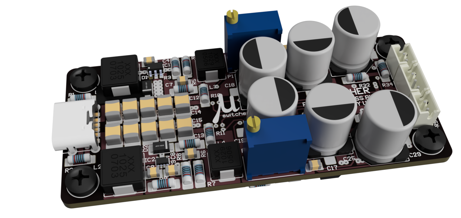
Fig.2: install the parts on the PC board as shown here, taking care
to ensure that all polarised parts are correctly oriented. Also, make certain you use the correct transistor type at each location. Below is the completed PC board.
Bill of Materials
| Name | Value | Package | Quantity |
|---|
| R1,R2 | 5k1Ω | MELF0204 | 2 |
| R3 | 10kΩ | MELF0204 | 1 |
| R4 | 7k32Ω | MELF0204 | 1 |
| R5 | 100kΩ | MELF0204 | 1 |
| R6,R8 | 12kΩ | MELF0204 | 2 |
| R7 | 270kΩ | MELF0204 | 1 |
| R9 | 680Ω | MELF0204 | 1 |
| R10,R11 | 0Ω47 | MELF0204 | 2 |
| R12,R13,R16,R17 | 2k7Ω | MELF0204 | 4 |
| R14,R15 | 175Ω | MELF0204 | 2 |
| R18,R19,R20,R21,R24,R25,R32,R33,R34,R35 | 22Ω | MELF0204 | 10 |
| R22,R23 | 200kΩ | MELF0204 | 2 |
| R26,R27,R28,R29 | 735Ω | MELF0204 | 4 |
| R30,R31 | 5Ω6 | MELF0204 | 2 |
| D1,D2 | SBR3U40S1F-7 | SOD-123F | 2 |
| D3,D4,D5,D6,D7,D8,D9,D10,D11,D12 | MBRS1100T3 | SMB-2 | 10 |
| IC1 | LMR62421 | SOT23-5 | 1 |
| IC2 | TPS62933PDRLR | SOT583-8 | 1 |
| IC3 | LM317DCY | SOT223-4 | 1 |
| IC4 | LM337IMPX/NOPB | SOT223-4 | 1 |
| IC5,IC6 | ADA4898-1 | SOIC-8 | 2 |
| C1,C2,C3,C5,C12,C13,C14,C15 | 22µF/25V | 1210 | 8 |
| C4,C16,C17,C20,C21,C22,C23 | 22µF/25V | 0805 | 7 |
| C6,C26,C27 | 10nF/25V | 0805 | 3 |
| C7 | 2n7/25V | 0805 | 1 |
| C8 | 470nF/25V | 0805 | 1 |
| C9 | 220pF/25V | 0805 | 1 |
| C10,C11 | 22uF/25V | 1210 | 2 |
| C18,C19,C24,C25,C28,C29 | 220µF/25V | 8mm | 6 |
| P1,P2 | 1kΩ | 3296W | 2 |
| L1,L2 | 10µH/4A | 6.6x3x7.3 | 2 |
| L3,L4 | 3µ3H/5A | 5.2x3x5.4 | 2 |
| V+,GND,V- | B3B-ZR-3.4(LF)(SN) | 3-PIN | 1 |
| RS+, RS- | B2B-ZR-3.4(LF)(SN) | 2-PIN | 2 |
| USB1 | USB4125-GF-A-0190 | TYPE-C | 1 |
| SCREW1-4 | M2.5x6 | SCREW | 4 |
Download
- OME uSwitcher PSU - Schematic (PDF)0
Sipi Shunt PSU
![]()
High Class Shunt PSU
SIPI SHUNT psu is designed to be applied as an upgrade in analog and digital playback equipment like (SA)CD players, DACs, PREAMPs and alike. The shunts drop in instead of commonly used industrial types of regulators. Having much lower noise, true wide bandwidth and linear output impedance, they’ll bring improvement to sound in terms of:
- higher resolution
- better transparency
- clean low ends
- increased dynamics
Traditionally, voltage regulators never where designed for audio applications. As an example, the very popular 7805 initially was designed as a voltage regulator for digital logic and low micro controllers - who cared about bandwidth or output noise. Derrivatives like 7815 and 7915 are widely used to supply the analogue output stage of CD players. About time for an upgrade!
Why Shunt?
The shunts consist of an active wide band current source to isolate the input from the output. The output is regulated by an active shunt regualtor with both low output noise and wide active bandwidth. For RF frequencies using the shunts is also beneficial in terms of additional decoupling: All output electrolytics can be left out!
Circuit details
At input AC connectors we have CRC filter that is used to suppress toroidal “ringing”, so we need to only find R1 and R2 value using “Quasimodo” test jig to get lowest “ringing” as possible. If you don’t have testing jig you can use default 150Ω as starting value. Next circuit is a full wave bridge rectifier that is used to convert AC sinusoidal voltage to DC voltage, and we have used here MBR1100 Shottky Diode that have fast turn ON/OFF recovery time with low dropout voltage.
After full wave rectifier there is a RCC filter that “surpress” noise generated from rectifier and that comes from AC voltage outlet. If you have few volts larger DC voltage that will be come to our shunt regulator you can increase or decrease these resistor values in RCC filter.
Rectified and filtered DC voltage is then feed to Constant Current Source (Q1 & Q4) that is limiting current at output. Reference voltage for CCS is RED LED that have forward voltage of 1,7V. Using resistors (R7 & R8) we set maximum current that will be available at the output using formula R=1V/limiting current. So we set our CCS to be limiting current of about 66mA. Our shunt gets about 25mA-30mA to function correctly, so output available current for load is about 40mA. If you need larger value you can decrease resistors (R7 & R8) to get larger available current for load.Max output current is 100mA available for load (plus 25mA-30mA for shunt themself to function correctly). LED biasing current is about 2-3mA and is set using JFET connected as CCS, and it’s current is set using resistors (R10 & R12).
Because AC filtering capacitor for shunt is large value (C15 & C16) ie 47uF we use simple BJT and zener that at startup it fast charges capacitors (C15 & C16), and after these capacitors is fully charge BJT and zener is inactive. This allows us to get fast startup below 1 seconds, without them startup will be around 5-6seconds.
Next circuit is our shunt reference TL431 that is used to set reference voltage for output shunt element (Q9 & Q10), using trimmer (P1 & P2) we can set output voltage for our load which controls shunt elements (Q9 & Q10). Here is one exceptional note that in positive and negative rail we have our shunt BJT connected collector to virtual ground, this way we get better shunt current control and better transient response at output.
Because our shunt element is away from our load, we implement remote sense connectors that connect to load. This way we have same performanse on load like that shunt regulator is on load PCB.Keep in mind that maximum remote sense wires and force wires (V+ GND V-) is maximum 10cm or less.
Output bypass capacitors 47μF (C19 & C20) needs to be non Low ESR type. If you put low ESR capacitors at output you will maybe get oscillations. So put here normal capacitors to get stable output.
Shunt regulators needs to be put on heatsink that have temperature resistance 5 K/W or less, to avoid overheating output shunt regulators. After shunt psu is build connect resistors between (V+ & GND) and (V- & GND) to simulate current draw. Without load at output all available current that is set using CCS will be burn on output shunts and there will be very high dissipation.
We calculate resistors using formula R=output voltage/load current. So in our example R=24V/40mA we set at output 600Ω resistors(choose nearest lower resistor value), and power rating for resistors is calculated using formula P=I^xR, so power rating will be 40mA^x600Ω is around 1W, we put 2W minimum resistor rating.
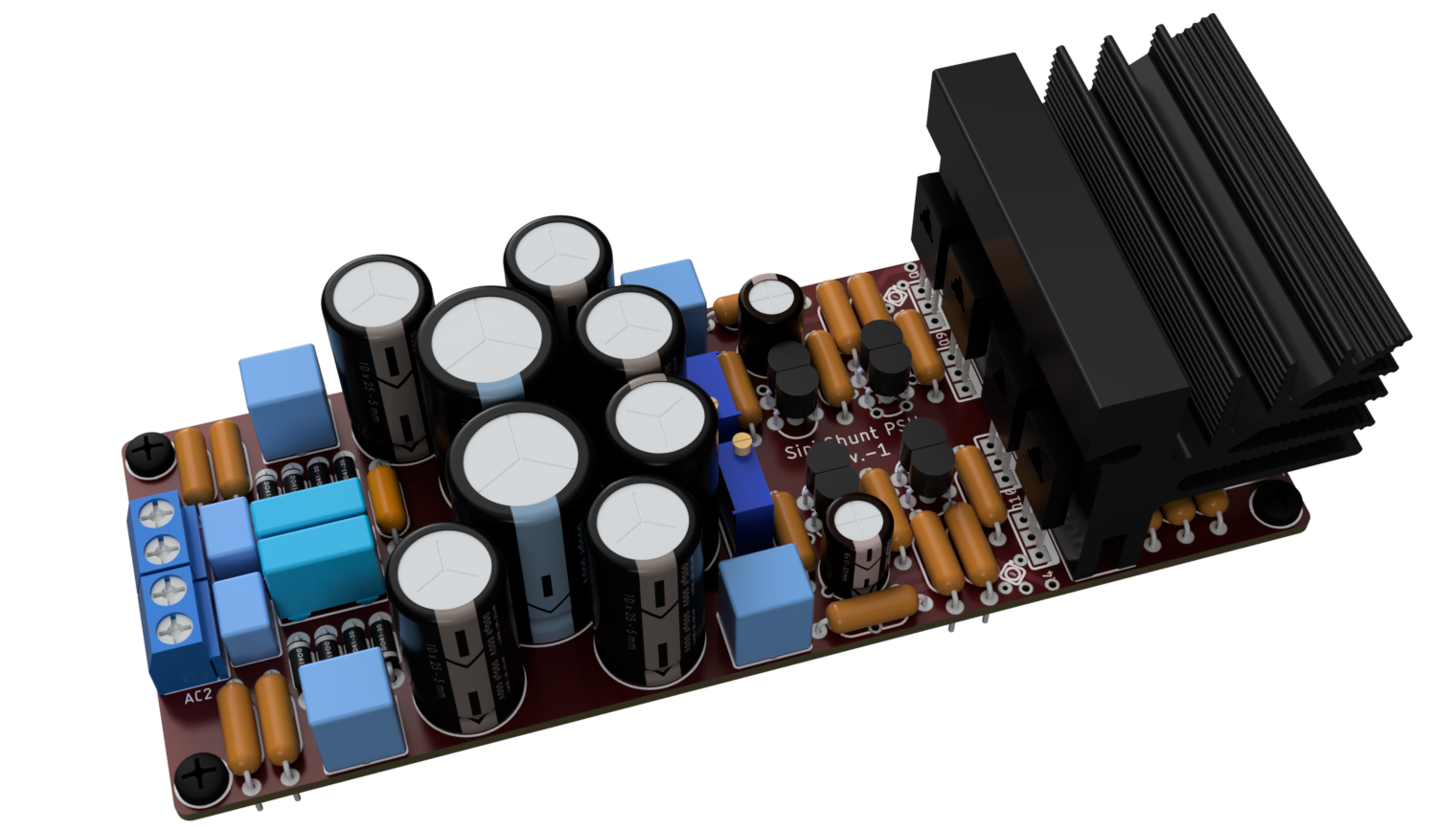
Fig.2: install the parts on the PC board as shown here, taking care
to ensure that all polarised parts are correctly oriented. Also, make certain you use the correct transistor type at each location. Below is the completed PC board.
Bill of Materials
| Name | Value | Quantity |
|---|
| R1,R2 | 150Ω | 2 |
| R3,R4,R5,R6 | 4Ω7 | 4 |
| R7,R8,R22,R24 | 15Ω | 4 |
| R9,R11 | 3k3Ω | 2 |
| R10,R12,R17,R18 | 150Ω | 4 |
| R13,R14 | 120kΩ | 2 |
| R15,R16 | 2k2Ω | 2 |
| R19,R20 | 1kΩ | 2 |
| R21,R23 | 120Ω | 2 |
| Q1,Q9 | BD140-16 | 2 |
| Q4,Q10 | BD139-16 | 2 |
| Q2,Q3 | J113 | 2 |
| Q5,Q6,Q7,Q8 | 2N5401 | 4 |
| D1,D2,D3,D4,D5,D6,D7,D8 | MBR1100 | 8 |
| D9,D10 | BZX85C15 | 2 |
| IC1,IC2 | TL431 | 2 |
| C1,C2 | 10nF | 2 |
| C3,C4 | 150nF | 2 |
| C5,C6,C13,C14 | 100nF/100V/MKP | 4 |
| C7,C8,C11,C12 | 220μF/50V | 4 |
| C9,C10 | 2200μF/50V | 2 |
| C15,C16 | 47μF/50V | 2 |
| C17,C18 | 470μF/35V | 2 |
| C19,C20 | 47μF/35V | 2 |
| P1,P2 | 25kΩ | 2 |
| LED1,LED2 | HLMP6000 | 2 |
| AC1,AC2,V+,V- | KF301-2P | 4 |
| SENSE+,SENSE- | JST-XH2.54-2 | 2 |
| SCREW1-4 | M3 | 4 |
Download
- Sipi Shunt PSU - Schematic (PDF)0
- Sipi Shunt PSU - Layout (PDF)0
- Sipi Shunt PSU - PCB (PDF)0