OME FlatBT
High Class Audiophile Grade LINE Preamplifier
FlatBT is our answer to the growing demand for high-end preamplifiers from the audiophile and DIY community. In most cases, audiophiles look for linear stages with wide bandwidth and flat frequency response without any tone controls, as well as with very low output impedance for easy connection to modern output amplifiers. FlatBT was designed following such requirements and we believe that it will more than meet all reasonable expectations of even the most discerning and demanding audiophiles.
This preamp was designed using high quality components and professionally routed PCB board so that we get easy pcb assembly and high end specification of finished preamp device. We wrote this guide to be easy and understandable to DIY builders so you will get all informations from here.
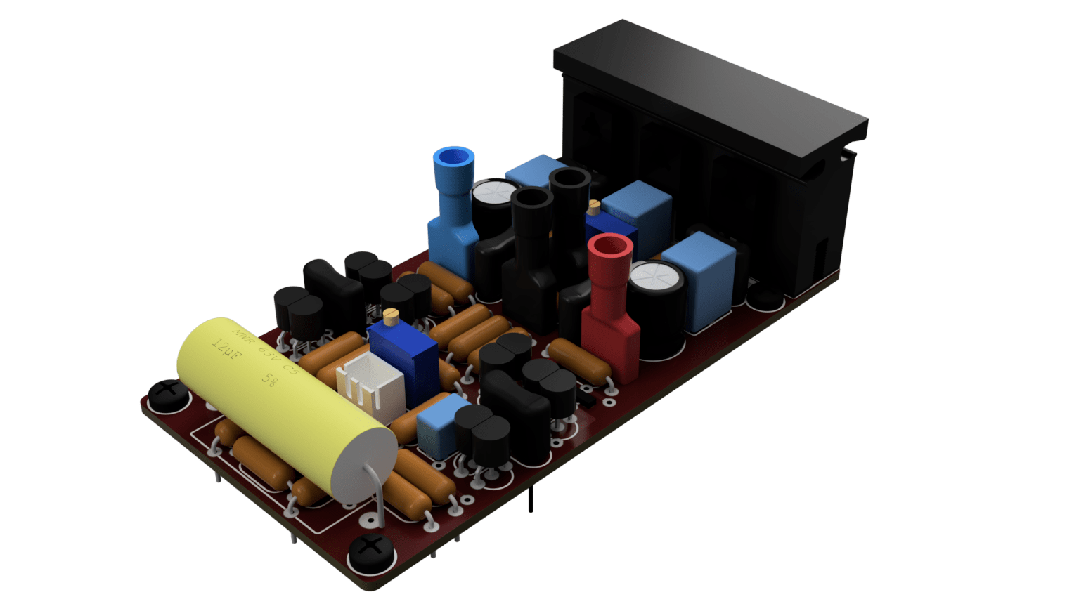
Before you start working, we recommend that you familiarize yourself first with the scheme, the layout of the parts and the pcb layout itself. This may seem trivial to the more experienced, but it has proven to be very useful for less experienced self-builders. We assume and expect that you are quite capable of: distinguishing and recognizing various components and reading their values, and that you skillfully use a soldering iron and soldering technique. If this is not the case, we ask and advise you to ensure the presence and help of someone with sufficient knowledge and practical experience during work! In order to successfully assemble this PREAMP, we advise you to strictly follow the drawing of the layout of the components as well as the order of the assembly stages as described below. The drawing of the layout of the parts on the plate is given as a “side view of the components”.
Assembling
It is best to start the assembly by placing the wire jumpers and then by placing the passive components. Generally speaking, it is very important to install all the components so that they have the shortest possible leads, which means that they should be placed so that they literally lie in contact with the surface of the pcb. Start by placing and soldering the resistors, then solder the two multi-turn trimmers and then install all the capacitors except the electrolytic ones. For all the components installed so far, it is completely unimportant how you turned them because they do not belong to the so-called “polarized” components. However, in the following stages, you will install components where it is VERY important how you turned them! The next step is to install the electrolytic capacitors, the polarity of which is always clearly indicated on the housing, usually by marking the negative pole. Place them according to these markings, but it is always recommended that before you solder them, you should check once again whether you have turned them correctly in terms of polarity.
After the electrolyte, it’s the turn of the “active” components, which are semiconductors, i.e. transistors and diodes. Try to do the soldering of semiconductors as quickly as possible, but still with high quality, because this type of component does not tolerate such high temperatures for a long period of time. These components are also “polarized” and it is very important how you turn them and which pin goes into which hole on the circuit board. If you make a mistake here, it is very possible that this component will be instantly destroyed at the moment of switching on, and it is almost certain that your device will not work. Incorrect installation of one component can cause the burning of some others that are already installed correctly! There are two LED diodes on the board. The LED has one leveled surface on the housing, and the pin that is closer to that surface is the cathode and is soldered to the square pad below the LED symbol on the board. All the small transistors in the TO92 case are placed so that their bottom is the surface away from the tile about 2-3mm … no more. Before placing and soldering them, form their legs so that their spacing matches the holes in which they are placed on the board.
Three more components remain to be installed. They are slightly larger transistors in a flat rectangular plastic case with a hole, and you need to solder them with the markings facing up. They should also be mechanically attached to a metal surface for cooling, as they heat up moderately during operation. A small cooler or a piece of 2-3mm thick aluminum sheet bent in the shape of the letter Z, which is attached to the lower cover of the preamp case, will be sufficient for this. We leave the final solution to you to adapt it to your wishes and the available space in the device.
Adjusting
ADJUSTING the preamplifier is very simple. First, check whether the circuit with which you will power the preamplifier provides the necessary and correct voltages that do not deviate more than 100-200mV from each other. Ideally, the positive and negative supply voltages should be identical, but it is much more important that they are the same than that they are exactly 24V. If this condition is met, complete the other connections of ONLY ONE channel of the preamp with the power supply. Now place the jumper on the input of the preamp and leave the output “open”, i.e. not connected anywhere. You should have two multimeters handy, but even one will do if you can’t do anything else. Set the switch on the multimeter to the 1 or 2V DCV range and place the test leads to measure the voltage across resistor R19. The red tip goes to the terminal of R19 that goes to the emitter of Q14 and the black tip to the other terminal that goes to the output. Turn on the power and observe what the instrument reads. Adjust the BIAS trimmer P2 until the instrument reads 450mV (0.45V). Now move the test leads of the instrument so that the red one is at the output of the preamp (connection R19 and R20) and the black one is at the ground of the power supply. Also change the measuring range of the instrument to the 100-200mV DCV position and adjust P1 so that the instrument reads 0V or as close to it as possible. Check again the voltage drop at R19, which should still be 450mV, and then check that there is still no DC voltage at the output. If necessary, adjust the corresponding trimmers P1&P2 a little more to achieve the required values. Repeat this same procedure with the board of the second channel and if everything is OK there, your preamplifier is ready to work!
Customizing
CUSTOMIZING this preamplifier is easy to do and should be done when there is a need for it in your setup due to some specifics. With the values of the elements given in the bill of materials, the total gain of FlatBT is set to 5x (five times) and is determined by the ratio of the resistances of R12 and R13 and according to the simple formula GAIN=(R13+R12)/R12. If your signal source (for example, a CD-player) gives a relatively high level at the output, the preamp gain may be too high for your setup, and this may lead to a decrease in the general sound quality of your system and an increase in distortion. To reduce the gain, you need to replace R12 (now 1.2k=1k2=1200ohm) with a higher resistance resistor. To reduce to 4x, put R12=1k6 and to reduce to 3x, put R12=2k4. If you have the opposite situation and need more gain, the procedure is also simple… just reduce the value of resistor R12 using the above formula.
Fig.2: install the parts on the PC board as shown here, taking care to ensure that all polarised parts are correctly oriented. Also, make certain you use the correct transistor type at each location. Below is the completed PC board.
Bill of Materials
| Name | Value | Quantity |
|---|---|---|
| R1 | 47kΩ | 1 |
| R2 | 120Ω | 1 |
| R3,R6,R18,R19 | 10Ω | 4 |
| R4,R5 | 18kΩ | 2 |
| R7 | 1kΩ | 1 |
| R8 | 4k7Ω | 1 |
| R9 | 240Ω | 1 |
| R10,R11 | 680Ω | 2 |
| R12 | 390Ω | 1 |
| R13,R20,R21 | 220Ω | 3 |
| R14,R15 | 18Ω | 2 |
| R16 | 2k4Ω | 1 |
| R17 | 2k7Ω | 1 |
| R22 | 33Ω | 1 |
| R23,R24 | 68Ω | 2 |
| R25,R26 | 15Ω | 2 |
| Q1,Q2,Q3,Q4,Q10,Q11,Q12 | KSC1845 | 7 |
| Q5,Q6,Q7,Q8,Q9 | KSA992 | 5 |
| Q13,Q14 | KSC3503 | 2 |
| Q15 | KSA1381 | 1 |
| C1 | 2μ2F/MCAP-250 | 1 |
| C2 | 150pF/MICA | 1 |
| C3 | 1n5F/KP1830 | 1 |
| C4,C5,C6 | 22pF/MICA | 3 |
| C7,C10,C11 | 100nF/MKP1837 | 3 |
| C8,C9 | 220μF/35V | 2 |
| C12,C13 | 47pF/MICA | 2 |
| LED1,LED2 | HLMP6000 | 2 |
| V+,GND, V-, SPK | 1-726388-2 | 4 |
| INPUT | JST-XH2.54-2 | 1 |
| H1 | SK492-50-8.5K/W | 1 |
| SCREW1-4 | M3 | 4 |
Download
- OME FlatBT - Schematic (PDF)0
- OME FlatBT - Layout (PDF)0
- OME FlatBT - PCB (PDF)0