OME MODUS
High Class Audio Power Amplifier
Power output is 100 watts RMS into a 8Ω load and 140 watts into 4Ω load, before the onset of clipping. A particular feature of the MODUS is low distortion.
Circuit description
Now let’s have a look at the circuit of Fig.1. 16 transistors and two diodes make up the semiconductor complement.
The input signal is coupled via a 2,2µF polypropylene capacitor (MKP) and 470Ω resistor to the base of Q1. Q1 & Q2 make up a differential pair. Q3 & Q4 is a constant current source which sets the current through Q1 & Q2 and renders the amplifier largely insensitive to variations in its supply rails (power supply rejection).
Signals from the collectors of Q1 & Q2 drive another differential pair, Q8 & Q9 which have a “current mirror” as their collector loads. The current mirror, comprising Q7 , ensure that this second differential stage has high linearity (ie, low distortion).
The output of Q6 & Q9 is then used to drive class-AB output stage consisting of drivers Q11 & Q12 and power transistors Ql3, Ql4, Q15 & Q16.
Q10 is a Vbe multiplier, so-called because it multiplies the voltage between its base and emitter to provide a fixed voltage between its collector and emitter, regardless of the drive current delivered to the output stage by Q11 & Q12. The voltage is adjusted by trimpot BIAS.
The function of Q10 is to set the DC voltage applied between the bases of Q11 & Q12. By doing this it sets the “quiescent current” in the output stage (ie, the current when no signal is present). This is to minimise crossover distortion.
The complementary output transistors are connected in parallel to give high output current capability. Each transistor has its own 0.22Ω emitter resistor. These are included to ensure that the output current is shared reasonably well between the output transistors.
Negative feedback is applied from the output stage back to the base of Q2 via a 10kΩ resistor. The level of feedback, and therefore the voltage gain, is set by the ratio of the 10kΩ resistor to the 330Ω at the base of Q2. The 470µF bipolar capacitor in series with the 330Ω sets the DC gain to unity and sets the -3dB point of the frequency response to about 2Hz. The other determinant of the amplifier’s low frequency response is the 2,2µF input capacitor and the 10kΩ base bias resistor feeding Ql and these set a -3dB point at about 7Hz.
The 220pF capacitor together with the 10kΩ resistor feeding Q1 form a low pass filter to roll off frequencies above 200kHz.
Another important factor in the amplifier’s excellent stability is the output RLC network consisting of the 4,7µH choke, a 2,2Ω resistor and a 100nF capacitor with series 10Ω resistor. Not only does this network ensure stability but the capacitor is an effective killer of any RF and mains-interference signals which can he picked up by long loudspeaker leads.
PC Board Topology
As noted earlier, the design of the PC board is a very critical part of the overall circuit. The placement of the components and the way that heavy currents flow in the tracks is all arranged to minimise the radiation of harmonics into the input stage involving Ql & Q2.
This board is yet a further refinement of the topology we use and that is differential pair for input and vas stage, followed by Vbe multiplier with drivers that drives double emitter follower.
It incorporates “star earthing” whereby all earth currents come back to a central point on the board, thereby avoiding any flow of output, supply and bypass currents flowing in the signal earths.
Furthermore, placement of the copper tracks to the output stages is arranged, as far as possible, to cancel the magnetic fields produced by the asymmetric currents drawn by each half of the output stage.
By way of explanation, when the positive half of the output stage (Q13 & Q15) conducts, the DC current drawn is effectively a positive half wave (ie, rectification takes place) of the signal waveform, and when the negative half conducts (Ql4 & Q16), the DC current is the negative half wave.
A major cause of harmonic distortion in class-B amplifiers is the magnetic fields produced by these asymmetric currents inducing unwanted signals into the input stages, in this case involving Ql & Q2.
So we have tried to cancel these fields as much as possible (in a single sided PC board).
For example, notice how the heavy collector and emitter tracks placed close together. So what happens is that the magnetic field produced by the asymmetric current in collector tracks is more or less cancelled as the same current flows back in the emitter resistors.
It is then most important to arrange the DC supply cables to the amplifier to further this cancellation process.
To make the input stage less vulnerable to spurious magnetic fields from the output stage, we have concentrated it into as small an area of the PC board as possible.
Another trick is the location of the takeoff point for the 10kΩ resistor and its orientation at rightangles to the output stage emitter resistors.
Finally, the signal earth for the input stage is separated from the main amplifier earth by a 10Ω resistor. This is not so important when a single module is in use but it is most important when two modules are used in a stereo system.
In that situation, the joining of the two signal earths back via the input cables to a single program source such as a CD player will cause an earth loop and a resulting major degradation in the separation between channels and lesser degradation in the distortion performance.
Well, that’s probably enough discussion of the PC board but suffice to say that the overall design has been carefully arranged to minimise distortion and leave as little to chance in the wiring layout so that constructors are certain to get excellent results.
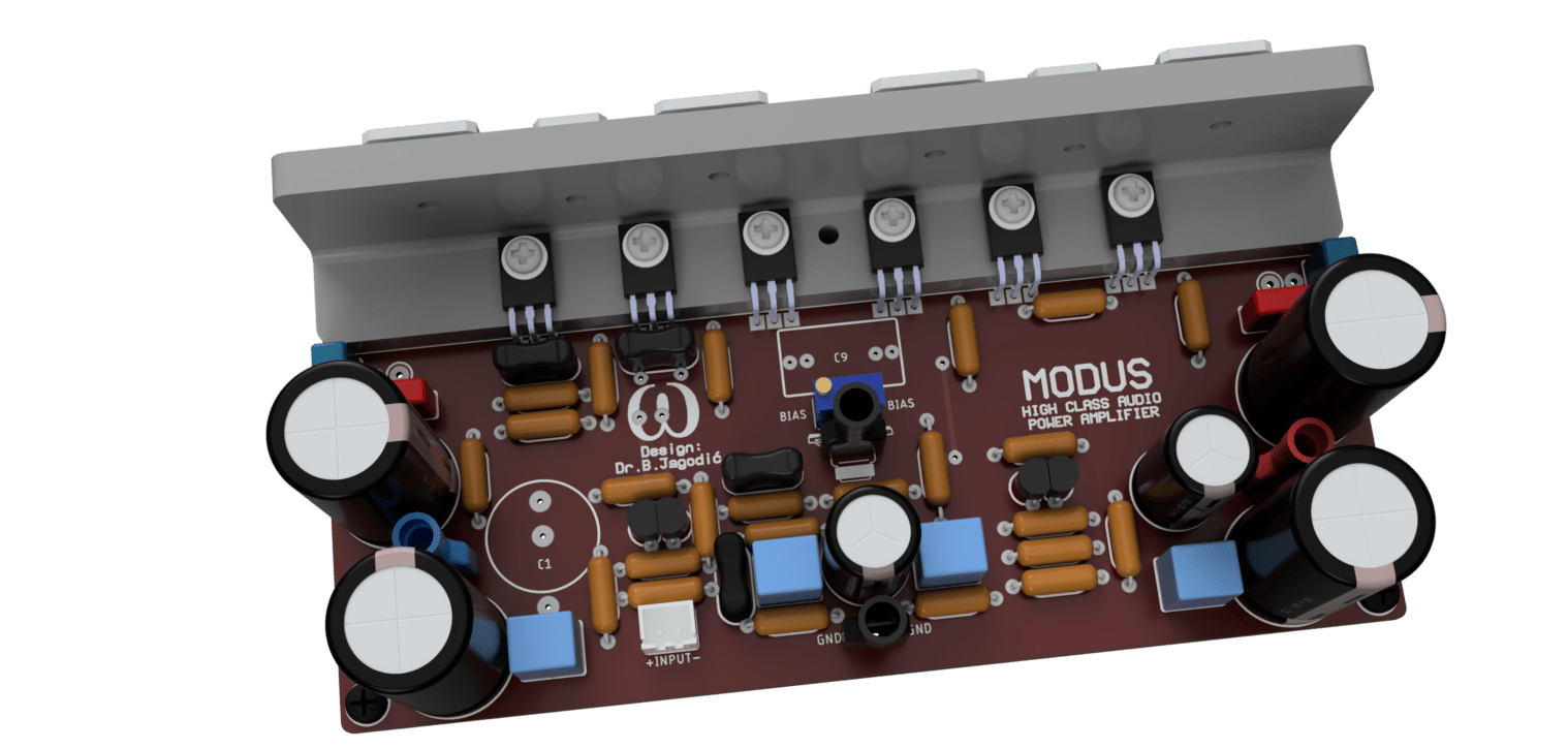
The PC board and the component placement is shown in Fig.2.
Fig.2: install the parts on the PC board as shown here, taking care to ensure that all polarised parts are correctly oriented. Also, make certain you use the correct transistor type at each location. Below is the completed PC board.
Bill of Materials
| Name | Value | Quantity |
|---|---|---|
| R1 | 470Ω | 1 |
| R2,R7,R15 | 10kΩ | 3 |
| R3,R35 | 10Ω/1W | 2 |
| R4 | 180Ω | 1 |
| R5 | 1kΩ | 1 |
| R6,R24,R25 | 47Ω | 1 |
| R8,R9 | 15kΩ | 2 |
| R10 | 8,2kΩ | 1 |
| R11,R12 | 22Ω | 2 |
| R13,R14,R22 | 1,8kΩ | 2 |
| R16 | 330Ω | 1 |
| R17,R18 | 100Ω | 2 |
| R19,R20 | 10Ω | 2 |
| R21 | 150Ω | 1 |
| R23 | 4,7kΩ | 1 |
| R26 | 33Ω/2W | 1 |
| R27,R28,R29,R30 | 2,2Ω | 4 |
| R31,R32,R33,R34 | 0,22Ω/5W | 4 |
| R36,R37 | 1Ω/2W | 2 |
| Q1,Q2,Q3,Q4 | KSA992 | 4 |
| Q5,Q6,Q10 | KSA1381 | 3 |
| Q7,Q8,Q9 | KSC3503 | 3 |
| Q11 | MJE15032 | 1 |
| Q12 | MJE15033 | 1 |
| Q13,Q15 | NJW3281G | 2 |
| Q14,Q16 | NJW1302G | 2 |
| D1,D2 | 1N4007 | 2 |
| C1 | 4,7μF/MCAP250 | 1 |
| C2 | 220pF/Mica | 1 |
| C3 | 47μF/63V | 1 |
| C4,C8 | 15pF/Mica | 2 |
| C5 | 470μF/16V | 1 |
| C6,C10,C11 | 100nF/100V/MKP | 3 |
| C7 | 120pF/Mica | 1 |
| C9 | 1μF/63V/MKP417 | 1 |
| C12,C13,C19,C20 | 470μF/63V | 4 |
| C15,C16 | 220nF/MKT | 2 |
| C17,C18 | 470nF/MKT | 2 |
| BIAS | 500Ω | 1 |
| V+,V-,SPK, PGND | 1-726388-2 | 4 |
| SCREW1-4 | M3 | 4 |
Download
- OME MODUS - Schematic (PDF)0